
Education
Colored Bands in CVD-Grown Diamond
Srushti Tanti and Raju Jain

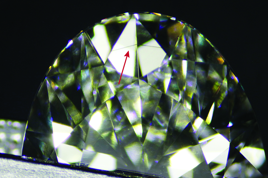
Figure 1. A growth remnant appeared as a color band (arrow) in a 3.14 ct CVD-grown diamond. Photomicrograph by Raju Jain; field of view ~11.75 mm.
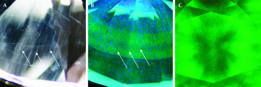
Figure 2. A: Hazy parallel lines (indicated by arrows) resembling whitish internal graining. Photomicrograph by Raju Jain; field of view ~6.31 mm. DiamondView imaging of the pavilion facets showed blue growth layers in green fluorescence (B), as well as strong green phosphorescence (C). Images by Suraj Maurya.
The Surat laboratory recently examined a 3.14 ct F-color oval brilliant diamond grown by chemical vapor deposition (CVD). The diamond featured a single dark brown band measuring ~2.2 mm in length that resembled graining in natural diamond (figure 1). The band was visible under the microscope as well as with a 10× loupe. The clarity grade was VVS2 based on this colored band, which was visible through multiple bezels and affected the transparency at that location. Through the pavilion, parallel whitish bands were also observed (figure 2A).
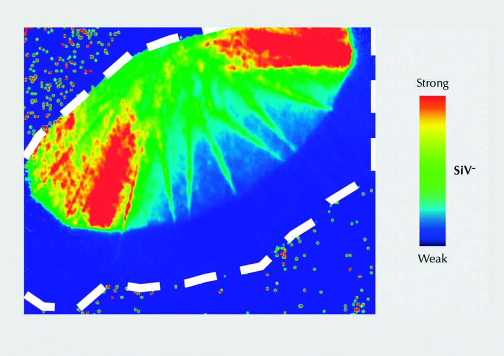
Figure 3. False-color PL map of the SiV– defect at 736.6/736.9 nm using 633 nm laser excitation, normalized to the diamond Raman area on the pavilion. The dashed line indicates the approximate outline of the diamond.
The subtle banding seen in this diamond differed from a cloud of graphite inclusions at a growth interface previously reported in a CVD-grown diamond (Summer 2023 Lab Notes, pp. 213–214). The fluorescence image collected by the DiamondView revealed a layered growth structure that did not coincide with the color banding, indicating a start-stop cycling growth process typical of CVD synthesis (figure 2B). Deep UV fluorescence with green and blue coloration as well as strong green phosphorescence seen in the DiamondView image (figure 2C) indicated high-pressure, high-temperature treatment. The SiV– defect at 736.6 and 736.9 nm, a common feature of CVD laboratory-grown diamond and only rarely seen in natural diamond, was observed in photoluminescence (PL) spectra using 457, 514, and 633 nm laser excitation. PL mapping (figure 3) revealed that the concentration of SiV– was higher near the culet of the pavilion and dramatically lower near the table.
GIA has documented growth remnants in thousands of CVD-grown diamonds. But with a multitude of manufacturers, recipes, and treatments, a wide variety of clarity characteristics are encountered, including the unusual color band observed here.
Authors: Srushti Tanti is an analytics technician, and Raju Jain is a training specialist, at GIA in Surat, India.
This article was contributed by GIA® (Gemological Institute of America®)
GIA.edu | GIAindia.in


Education
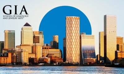
GIA To Open London Campus In August, Enrolling Students For Classes Beginning In August 2026
Campus in London’s Canary Wharf Will Place GIA Students In One Of The World’s Most Influential Centers For Luxury and Business.

The soon-to-open GIA (Gemological Institute of America) campus in London is now enrolling students for classes beginning in August 2026. The new GIA School of Gemology and Jewelry Arts campus in London’s Canary Wharf will place GIA students in one of the world’s most influential centers for luxury and business.
The new London campus in the iconic and vibrant Canary Wharf district will offer increased capacity and, for the first time in London, the GIA Jewelry Design & Technology program. The campus will be conveniently located near transport, cultural and social attractions. Historically, enrolment at GIA’s London campus has included students from more than 50 countries with unique and diverse backgrounds.
GIA President and CEO, Pritesh Patel said:

“GIA takes great pride in providing premier education through our programs. Our new London campus will allow us to further advance our mission to ensure confidence in gems and jewelry by making education more globally accessible and offering the highest quality gem and jewelry education.”
GIA’s London school was established in 2002, providing education in gemmology and jewellery design. The school is accredited by the British Accreditation Council (BAC) and Independent Schools Inspectorate (ISI).
-

 National News6 hours ago
MCX Gold, Silver Futures For August Delivery Rise On Renewed Geopolitical Tensions
-

 International News2 hours ago
Precious Metals Bounce Back As Iran Ceasefire Hopes Rise, But Fed Rate Fears Loom: AUGMONT BULLION REPORT
-
 National News3 hours ago
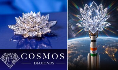
Cosmos Diamonds Makes History With World’s First LGD Jewellery Launched Into Space
-
 International News6 hours ago
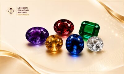
London Diamond Bourse Announces Launch Of Its New Coloured Gemstone Course